- 您现在的位置:买卖IC网 > Sheet目录1917 > DSPIC30F4011-30I/ML (Microchip Technology)IC DSPIC MCU/DSP 48K 44QFN
2010 Microchip Technology Inc.
DS70135G-page 115
dsPIC30F4011/4012
17.2
I2C Module Addresses
The I2CADD register contains the Slave mode
addresses. The register is a 10-bit register.
If the A10M bit (I2CCON<10>) is ‘0’, the address is
interpreted by the module as a 7-bit address. When an
address is received, it is compared to the 7 LSbs of the
I2CADD register.
If the A10M bit is ‘1’, the address is assumed to be a
10-bit address. When an address is received, it will be
compared with the binary value, ‘11110
A9
A8
’
(where A9 and A8 are two Most Significant bits of
I2CADD). If that value matches, the next address will
be compared with the Least Significant 8 bits of
I2CADD, as specified in the 10-bit addressing protocol.
The 7-bit I2C slave addresses supported by the
dsPIC30F are shown in Table 17-1.
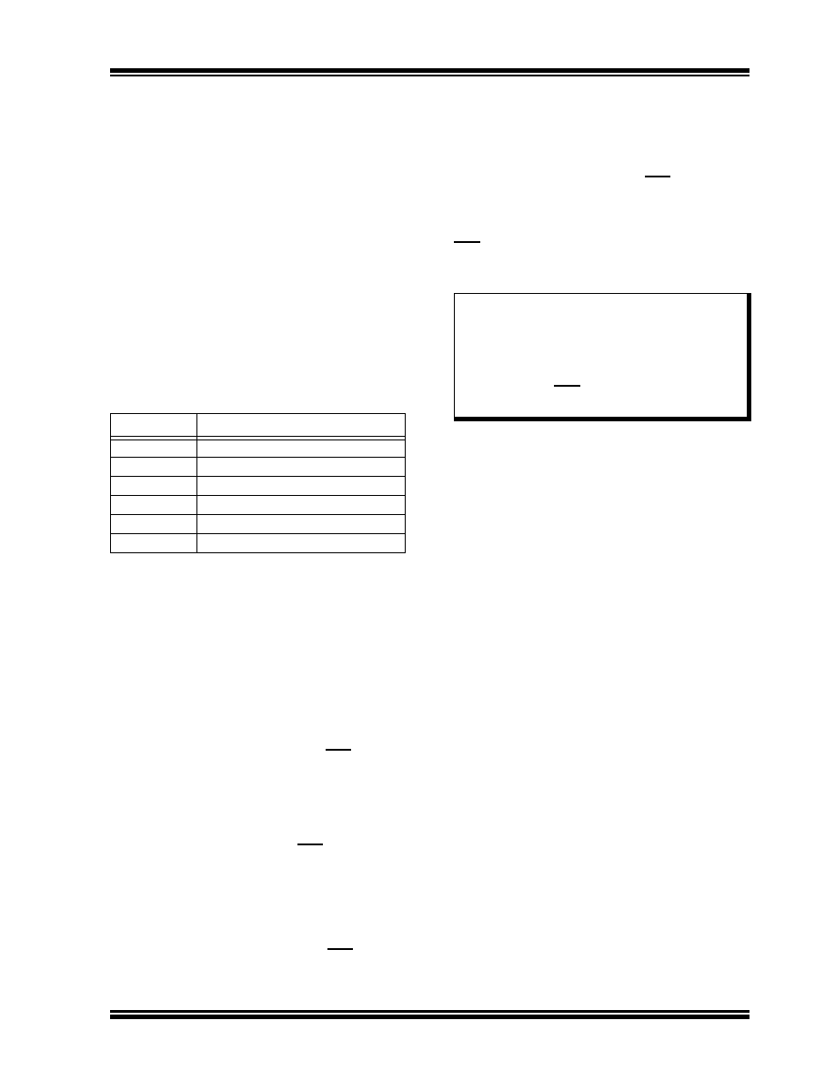
TABLE 17-1:
7-BIT I2C SLAVE
ADDRESSES
17.3
I2C 7-bit Slave Mode Operation
Once enabled (I2CEN = 1), the slave module will wait
for a Start bit to occur (i.e., the I2C module is ‘Idle’).
Following the detection of a Start bit, 8 bits are shifted
into I2CRSR and the address is compared against
I2CADD. In 7-bit mode (A10M = 0), I2CADD<6:0> bits
are compared against I2CRSR<7:1>, and I2CRSR<0>
is the R_W bit. All incoming bits are sampled on the
rising edge of SCL.
If an address match occurs, an Acknowledgement will
be sent, and the Slave Event Interrupt Flag (SI2CIF) is
set on the falling edge of the ninth (ACK) bit. The
address match does not affect the contents of the
I2CRCV buffer or the RBF bit.
17.3.1
SLAVE TRANSMISSION
If the R_W bit received is a ‘1’, then the serial port will
go into Transmit mode. It will send ACK on the ninth bit
and then hold SCL to ‘0’ until the CPU responds by writ-
ing to I2CTRN. SCL is released by setting the SCLREL
bit and 8 bits of data are shifted out. Data bits are
shifted out on the falling edge of SCL, such that SDA is
valid during SCL high (see timing diagram). The inter-
rupt pulse is sent on the falling edge of the ninth clock
pulse, regardless of the status of the ACK received
from the master.
17.3.2
SLAVE RECEPTION
If the R_W bit received is a ‘0’ during an address
match, then Receive mode is initiated. Incoming bits
are sampled on the rising edge of SCL. After 8 bits are
received, if I2CRCV is not full or I2COV is not set,
I2CRSR is transferred to I2CRCV. ACK is sent on the
ninth clock.
If the RBF flag is set, indicating that I2CRCV is still
holding data from a previous operation (RBF = 1), then
ACK is not sent; however, the interrupt pulse is gener-
ated. In the case of an overflow, the contents of the
I2CRSR are not loaded into the I2CRCV.
17.4
I2C 10-bit Slave Mode Operation
In 10-bit mode, the basic receive and transmit
operations are the same as in the 7-bit mode. However,
the criteria for address match is more complex.
The I2C specification dictates that a slave must be
addressed for a write operation, with two address bytes
following a Start bit.
The A10M bit is a control bit that signifies that the
address in I2CADD is a 10-bit address rather than a
7-bit address. The address detection protocol for the
first byte of a message address is identical for 7-bit
and 10-bit messages but the bits being compared are
different.
I2CADD holds the entire 10-bit address. Upon receiv-
ing an address following a Start bit, I2CRSR<7:3> is
compared against a literal ‘11110’ (the default 10-bit
address) and I2CRSR<2:1> are compared against
I2CADD<9:8>. If a match occurs and if R_W = 0, the
interrupt pulse is sent. The ADD10 bit will be cleared to
indicate a partial address match. If a match fails or
R_W = 1, the ADD10 bit is cleared and the module
returns to the Idle state.
The low byte of the address is then received and com-
pared with I2CADD<7:0>. If an address match occurs,
the interrupt pulse is generated and the ADD10 bit is
set, indicating a complete 10-bit address match. If an
address match did not occur, the ADD10 bit is cleared
and the module returns to the Idle state.
Address
Description
0x00
General call address or Start byte
0x01-0x03
Reserved
0x04-0x07
HS mode master codes
0x08-0x77
Valid 7-bit addresses
0x78-0x7B
Valid 10-bit addresses (lower 7 bits)
0x7C-0x7F
Reserved
Note:
The I2CRCV will be loaded if the I2COV
bit = 1 and the RBF flag = 0. In this case,
a read of the I2CRCV was performed but
the user did not clear the state of the
I2COV
bit
before
the
next
receive
occurred. The Acknowledgement is not
sent (ACK = 1) and the I2CRCV is
updated.
发布紧急采购,3分钟左右您将得到回复。
相关PDF资料
DSPIC30F4013-30I/ML
IC DSPIC MCU/DSP 48K 44QFN
DSPIC30F5013-30I/PT
IC DSPIC MCU/DSP 66K 80TQFP
DSPIC30F5015-30I/PT
IC DSPIC MCU/DSP 66K 64TQFP
DSPIC30F6010-20E/PF
IC DSPIC MCU/DSP 144K 80TQFP
DSPIC30F6010A-30I/PF
IC DSPIC MCU/DSP 144K 80TQFP
DSPIC30F6013A-30I/PF
IC DSPIC MCU/DSP 132K 80TQFP
DSPIC30F6014-30I/PF
IC DSPIC MCU/DSP 144K 80TQFP
DSPIC33EP512MU814-I/PL
IC DSC 16BIT 512KB 144LQFP
相关代理商/技术参数
DSPIC30F4011-30I/P
功能描述:数字信号处理器和控制器 - DSP, DSC 16bit Signal Cntrlr RoHS:否 制造商:Microchip Technology 核心:dsPIC 数据总线宽度:16 bit 程序存储器大小:16 KB 数据 RAM 大小:2 KB 最大时钟频率:40 MHz 可编程输入/输出端数量:35 定时器数量:3 设备每秒兆指令数:50 MIPs 工作电源电压:3.3 V 最大工作温度:+ 85 C 封装 / 箱体:TQFP-44 安装风格:SMD/SMT
DSPIC30F4011-30I/PT
功能描述:数字信号处理器和控制器 - DSP, DSC 16 Bit MCU/DSP 30M 48KB FL RoHS:否 制造商:Microchip Technology 核心:dsPIC 数据总线宽度:16 bit 程序存储器大小:16 KB 数据 RAM 大小:2 KB 最大时钟频率:40 MHz 可编程输入/输出端数量:35 定时器数量:3 设备每秒兆指令数:50 MIPs 工作电源电压:3.3 V 最大工作温度:+ 85 C 封装 / 箱体:TQFP-44 安装风格:SMD/SMT
DSPIC30F4011T-20E/ML
功能描述:数字信号处理器和控制器 - DSP, DSC 16 Bit MCU/DSP 44LD 20M 48KB FL RoHS:否 制造商:Microchip Technology 核心:dsPIC 数据总线宽度:16 bit 程序存储器大小:16 KB 数据 RAM 大小:2 KB 最大时钟频率:40 MHz 可编程输入/输出端数量:35 定时器数量:3 设备每秒兆指令数:50 MIPs 工作电源电压:3.3 V 最大工作温度:+ 85 C 封装 / 箱体:TQFP-44 安装风格:SMD/SMT
DSPIC30F4011T-20E/PT
功能描述:数字信号处理器和控制器 - DSP, DSC 16 Bit MCU/DSP 20M 48KB FL RoHS:否 制造商:Microchip Technology 核心:dsPIC 数据总线宽度:16 bit 程序存储器大小:16 KB 数据 RAM 大小:2 KB 最大时钟频率:40 MHz 可编程输入/输出端数量:35 定时器数量:3 设备每秒兆指令数:50 MIPs 工作电源电压:3.3 V 最大工作温度:+ 85 C 封装 / 箱体:TQFP-44 安装风格:SMD/SMT
DSPIC30F4011T-20I/ML
功能描述:数字信号处理器和控制器 - DSP, DSC DIG SIG CONTR RoHS:否 制造商:Microchip Technology 核心:dsPIC 数据总线宽度:16 bit 程序存储器大小:16 KB 数据 RAM 大小:2 KB 最大时钟频率:40 MHz 可编程输入/输出端数量:35 定时器数量:3 设备每秒兆指令数:50 MIPs 工作电源电压:3.3 V 最大工作温度:+ 85 C 封装 / 箱体:TQFP-44 安装风格:SMD/SMT
DSPIC30F4011T-20I/PT
功能描述:数字信号处理器和控制器 - DSP, DSC 16 Bit MCU/DSP 20M 48KB FL RoHS:否 制造商:Microchip Technology 核心:dsPIC 数据总线宽度:16 bit 程序存储器大小:16 KB 数据 RAM 大小:2 KB 最大时钟频率:40 MHz 可编程输入/输出端数量:35 定时器数量:3 设备每秒兆指令数:50 MIPs 工作电源电压:3.3 V 最大工作温度:+ 85 C 封装 / 箱体:TQFP-44 安装风格:SMD/SMT
DSPIC30F4011T-30I/ML
功能描述:数字信号处理器和控制器 - DSP, DSC 16 Bit MCU/DSP 44LD 30M 48KB FL RoHS:否 制造商:Microchip Technology 核心:dsPIC 数据总线宽度:16 bit 程序存储器大小:16 KB 数据 RAM 大小:2 KB 最大时钟频率:40 MHz 可编程输入/输出端数量:35 定时器数量:3 设备每秒兆指令数:50 MIPs 工作电源电压:3.3 V 最大工作温度:+ 85 C 封装 / 箱体:TQFP-44 安装风格:SMD/SMT
DSPIC30F4011T-30I/PT
功能描述:数字信号处理器和控制器 - DSP, DSC 16 Bit MCU/DSP 30M 48KB FL RoHS:否 制造商:Microchip Technology 核心:dsPIC 数据总线宽度:16 bit 程序存储器大小:16 KB 数据 RAM 大小:2 KB 最大时钟频率:40 MHz 可编程输入/输出端数量:35 定时器数量:3 设备每秒兆指令数:50 MIPs 工作电源电压:3.3 V 最大工作温度:+ 85 C 封装 / 箱体:TQFP-44 安装风格:SMD/SMT